Physical Design Mentorship

Why PD?

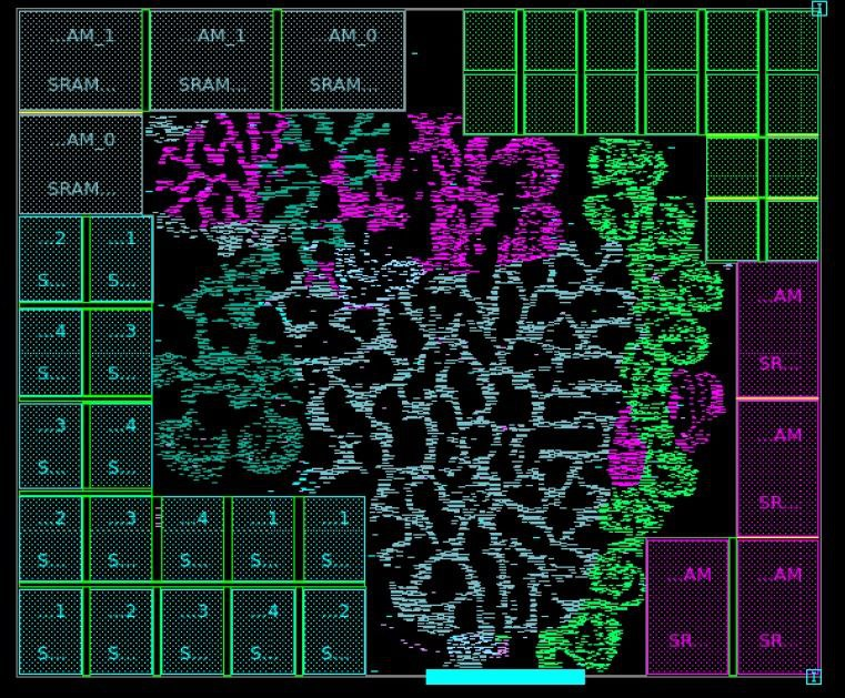
Physical Design is conversion of a set of gates connected through nets (netlist) to a layout form in a given chip area meeting aspects of power, area, performance (STA) honouring time to market. Floorplan, placement of cells, clock building, routing of metals connecting the logic gates and meeting the desired timing frequency is the goal of Physical Design.

Course overview - PD

20 weeks program

Program covers all aspects of RTL to GDSII flow (refer syllabus for integrated)

Every topic and sub-topic covers industry oriented practical aspects

Every topic and sub-topic is taught with hands-on lab from RTL to GDSII

In depth coverage of topics like Advanced Digital Design, CMOS, PnR flow, Pre-Layout STA and Sign-Off STA, Physical Verification, Low Power Methodologies, Logic Equivalence Check and TCL Scripting are key differentiators in the program

Curriculum and projects are co-developed with inputs from Industry experts

Soft skill training on the fly during the sessions

Resume preparation guidance

Regular assessment of areas where program members need improvement

Thorough in depth learning by interlinked theory and labs in parallel

Course completion certificate after completion of program

Trainers and Mentors available anytime for discussion

Path to VLSI industry will be clear once this program is completed

Labs can be accessed 24x7 through VPN from anywhere


ABOUT US

Trainer

Comes with 20+ years of industry experience.

Comes with 15+ years of training experience.

Successfully taped out 50+ designs.

Executed Full Chip, Sub-System and block levels creating partitions.

Have worked on Signoff like STA, Full-CHIP PV & IR etc.

Trained about 1000+ engineers worldwide.

Trainer has experience in leading a team of 60+ engineers.

Working on Full Chip and methodology development.

Technology node expertise from 5nm till 250nm across various foundries.

Strong hands on experience in Synopsys and Cadence tool sets.

Strong in TCL and PERL Scripting.

Syllabus - PD

Basics:

  •   Module 1: Digital Circuit Design
  •   Module 2: CMOS Circuit & Layout Design
  •   Module 3: Linux Operating System
  •   Module 4: ASIC/SOC Design flow
  •   Module 5: PDK and Technology Library
  •   Module 6: Standard Cell & Macro Libraries
  •   Module 7: Timing Constraint ( SDC ) Development
  •   Module 8: Static Timing Analysis

Implementation:

  •   Module 9: RTL Synthesis
  •   Module 10: Pre-Layout STA
  •   Module 11: Introduction to DFT
  •   Module 12: Introduction to Physical Design Flow
  •   Module 13: Design Planning (Floorplan)
  •   Module 14: Power-Routing
  •   Module 15: Physical Cells Placement & Std-Cell Pre-Placement
  •   Module 16: Std-Cell Placement
  •   Module 17: Scan-Chain Reordering
  •   Module 18: Pre-CTS Timing Analysis & Optimization
  •   Module 19: CTS
  •   Module 20: Post-CTS Timing Analysis & Optimization
  •   Module 21: Routing

Signoff Checks:

  •   Module 22: Physical Verification
  •   Module 23: RC Extraction
  •   Module 24: Sign-off STA Checks
  •   Module 25: Timing Closure
  •   Module 26: ECO Implementation
  •   Module 27: Logical Equivalence Check
  •   Module 28: IR-Drop and Electromigration Analysis Flow

Advanced Topics:

  •   Module 29: Low Power Methodologies & UPF
  •   Module 30: TCL Scripting
  •   Module 31: Advanced STA Topics
  •   Module 32: Introduction to Fin-FET & Double-Patterning.
  •   Module 33: Introduction to 16nm, 7nm Technologies & Floorplan Challenges
  •   Module 34: Make-Flow & LSF

Projects:

  •   Module 35: Final Projects ( Multiple Designs with different technologies )

Placement & Career Guidance:

  •   Soft-Skills Training
  •   Student Presentation
  •   Resume Preparation
  •   Interview Guidance
  •   Mock Interviews